- English
- Español
- Português
- русский
- Français
- 日本語
- Deutsch
- tiếng Việt
- Italiano
- Nederlands
- ภาษาไทย
- Polski
- 한국어
- Svenska
- magyar
- Malay
- বাংলা ভাষার
- Dansk
- Suomi
- हिन्दी
- Pilipino
- Türkçe
- Gaeilge
- العربية
- Indonesia
- Norsk
- تمل
- český
- ελληνικά
- український
- Javanese
- فارسی
- தமிழ்
- తెలుగు
- नेपाली
- Burmese
- български
- ລາວ
- Latine
- Қазақша
- Euskal
- Azərbaycan
- Slovenský jazyk
- Македонски
- Lietuvos
- Eesti Keel
- Română
- Slovenski
- मराठी
- Srpski језик
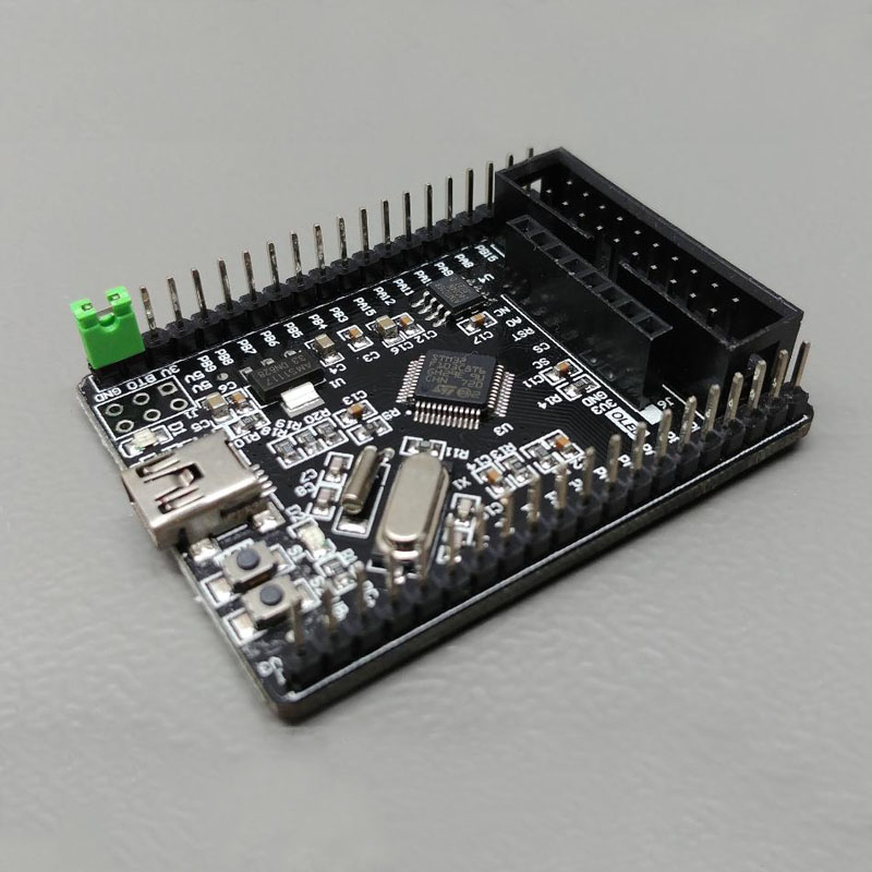
ARM STM32 MCU Board
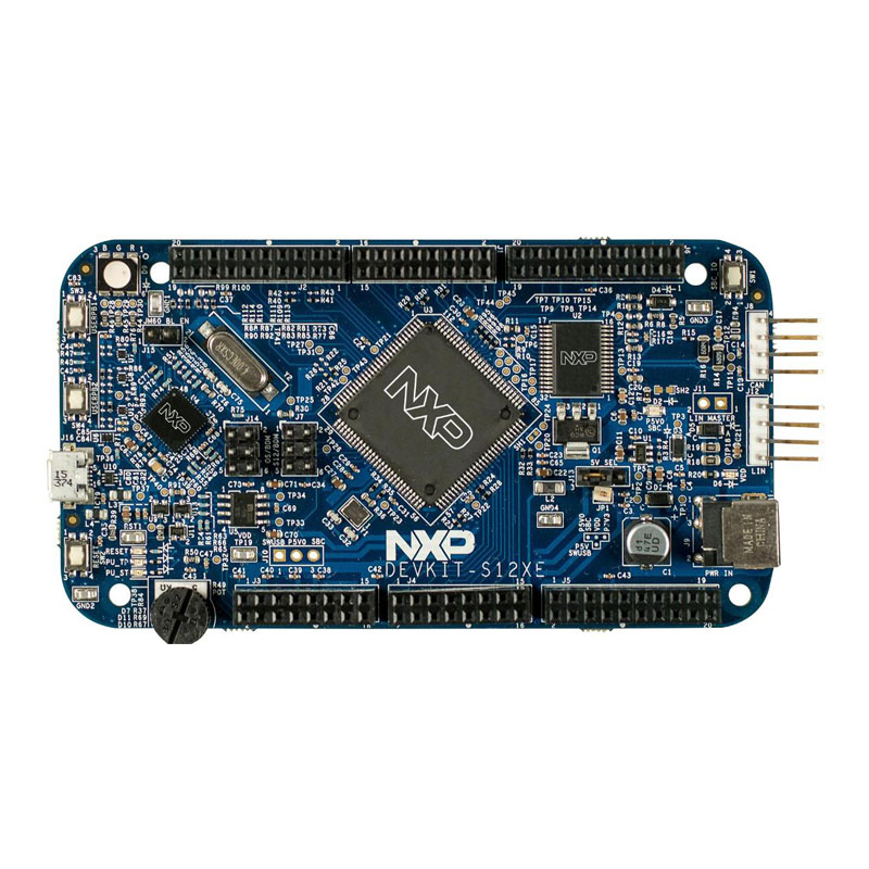
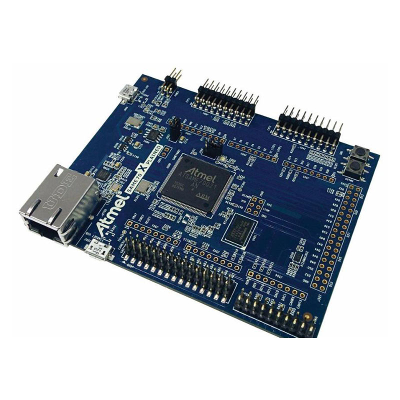
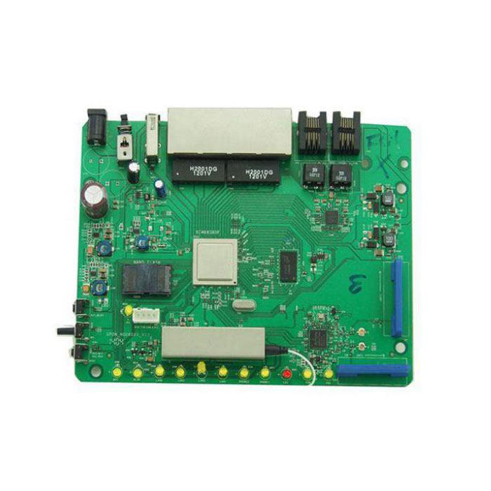
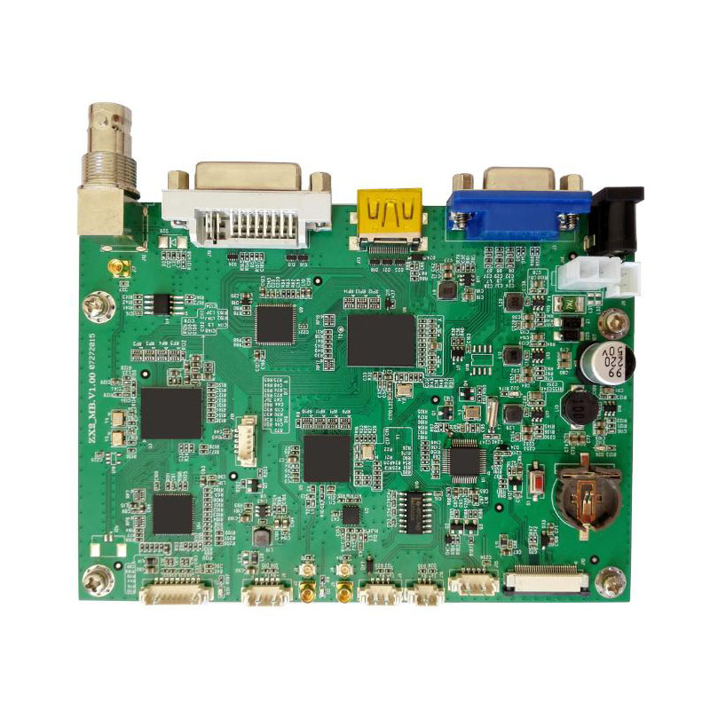
Ningbo Hi-tech Easy Choice Technology Co., Ltd is a high-tech company that is active in the design, development, and production of the ARM STM32 MCU Board. Our company's reputation is built on good credit and providing exceptional service, which has resulted in long-term collaborations with significant corporations, government agencies, and a wide user community.We specialize in intelligent electronic control board development, mechanical and electrical control product design, single-chip microcomputer development, circuit design, and post-production testing. We may custom-design the control circuit to satisfy your needs, enabling the fulfillment of your intended product functionalities, whether you supply explicit functional requirements or merely an idea.
Send Inquiry
YCTECH industrial product control board development includes industrial control board software design, software upgrade, schematic diagram design, PCB design, PCB production and PCBA processing located in the east coast of China. Our company designs, develops and manufactures ARM STM32 MCU board. Core: ARM32-bit Cortex-M3 CPU, the highest operating frequency is 72MHz, 1.25DMIPS/MHz. Single-cycle multiply and hardware divide.
Memory: On-chip integrated 32-512KB Flash memory. 6-64KB of SRAM memory.
Clock, reset and power management: 2.0-3.6V power supply and driving voltage for I/O interface. Power-on reset (POR), power-down reset (PDR), and programmable voltage detector (PVD). 4-16MHz crystal oscillator. Built-in 8MHz RC oscillator circuit adjusted before factory. Internal 40 kHz RC oscillator circuit. PLL for CPU clock. 32kHz crystal with calibration for RTC.
Low power consumption: 3 low power consumption modes: sleep, stop, standby mode. VBAT to power the RTC and backup registers.
Debug mode: serial debug (SWD) and JTAG interface.
DMA: 12-channel DMA controller. Supported peripherals: timers, ADC, DAC, SPI, IIC and UART.
Three 12-bit us-level A/D converters (16 channels): A/D measurement range: 0-3.6V. Dual sample and hold capability. A temperature sensor is integrated on-chip.
2-channel 12-bit D/A converter: STM32F103xC, STM32F103xD, STM32F103xE exclusive.
Up to 112 fast I/O ports: Depending on the model, there are 26, 37, 51, 80, and 112 I/O ports, all of which can be mapped to 16 external interrupt vectors. All but the analog inputs can accept inputs up to 5V.
Up to 11 timers: 4 16-bit timers, each with 4 IC/OC/PWM or pulse counters. Two 16-bit 6-channel advanced control timers: up to 6 channels can be used for PWM output. 2 watchdog timers (independent watchdog and window watchdog). Systick timer: 24-bit down counter. Two 16-bit basic timers are used to drive the DAC.
Up to 13 communication interfaces: 2 IIC interfaces (SMBus/PMBus). 5 USART interfaces (ISO7816 interface, LIN, IrDA compatible, debug control). 3 SPI interfaces (18 Mbit/s), two of which are multiplexed with IIS. CAN interface (2.0B). USB 2.0 full speed interface. SDIO interface.
ECOPACK package: STM32F103xx series microcontrollers adopt ECOPACK package.
system effect
1. ARM Cortex-M3 core integrated with embedded Flash and SRAM memory. Compared with 8/16-bit devices, ARM Cortex-M3 32-bit RISC processor provides higher code efficiency. STM32F103xx microcontrollers have an embedded ARM core, so they are compatible with all ARM tools and software.
2. Embedded Flash memory and RAM memory: Built-in up to 512KB embedded Flash, which can be used to store programs and data. Up to 64KB of embedded SRAM can be read and written at CPU clock speed (no wait states).
3. Variable static memory (FSMC): FSMC is embedded in STM32F103xC, STM32F103xD, STM32F103xE, with 4 chip selects, and supports four modes: Flash, RAM, PSRAM, NOR and NAND. 3 FSMC interrupt lines are connected to NVIC after OR. There is no read/write FIFO, except for PCCARD, codes are executed from external memory, Boot is not supported, and the target frequency is equal to SYSCLK/2, so when the system clock is 72MHz, external access is performed at 36MHz.
4. Nested Vectored Interrupt Controller (NVIC): It can handle 43 maskable interrupt channels (excluding 16 interrupt lines of Cortex-M3), providing 16 interrupt priorities. Tightly coupled NVIC achieves lower interrupt processing latency, directly transfers the interrupt entry vector table address to the kernel, tightly coupled NVIC kernel interface, allows interrupts to be processed in advance, handles higher priority interrupts that arrive later, and supports tail Chain, automatically saves the processor state, and the interrupt entry is automatically restored when the interrupt exits, without instruction intervention.
5. External interrupt/event controller (EXTI): The external interrupt/event controller consists of 19 edge detector lines for generating interrupt/event requests. Each line can be individually configured to select the trigger event (rising edge, falling edge, or both) and can be individually masked. There is a pending register to maintain the status of interrupt requests. EXTI is able to detect when a pulse on the external line is longer than the period of the internal APB2 clock. Up to 112 GPIOs are connected to 16 external interrupt lines.
6. Clock and start: It is still necessary to select the system clock when starting, but the internal 8MHz crystal oscillator is selected as the CPU clock when resetting. An external 4-16MHz clock can be selected and will be monitored for success. During this time, the controller is disabled and software interrupt management is subsequently disabled. At the same time, interrupt management of the PLL clock is fully available if required (eg in case of failure of an indirectly used crystal oscillator). Multiple pre-comparators can be used to configure the AHB frequency, including high-speed APB (PB2) and low-speed APB (APB1). The highest frequency of high-speed APB is 72MHz, and the highest frequency of low-speed APB is 36MHz.
7. Boot mode: At startup, the Boot pin is used to select one of the three Boot options: import from user Flash, import from system memory, and import from SRAM. The Boot import program is located in the system memory and is used to reprogram the Flash memory through USART1.
8. Power supply scheme: VDD, the voltage range is 2.0V-3.6V, the external power supply is provided through the VDD pin, which is used for I/O and internal voltage regulator. VSSA and VDDA, the voltage range is 2.0-3.6V, external analog voltage input for ADC, reset module, RC and PLL, within the range of VDD (ADC is limited to 2.4V), VSSA and VDDA must be connected to VSS accordingly and VDD. VBAT, the voltage range is 1.8-3.6V, when VDD is invalid, it supplies power for RTC, external 32KHz crystal oscillator and backup registers (realized by power switching).
9. Power management: The device has a complete power-on reset (POR) and power-down reset (PDR) circuit. This circuit is always effective to ensure that some necessary operations are performed when starting from 2V or falling to 2V. When VDD is below a specific lower limit VPOR/PDR, the device can also remain in reset mode without an external reset circuit. The device features an embedded programmable voltage detector (PVD). The PVD is used to detect VDD and compare it to the VPVD limit. An interrupt is generated when VDD is lower than VPVD or VDD is greater than VPVD. The interrupt service routine can generate a warning message or place the MCU in a safe state. PVD is enabled by software.
10. Voltage regulation: The voltage regulator has 3 operating modes: main (MR), low power consumption (LPR) and power down. MR is used in the regulation mode (running mode) in the traditional sense, LPR is used in stop mode, and power-down is used in standby mode: the voltage regulator output is high-impedance, the core circuit is powered down, including zero consumption (the contents of registers and SRAM are not will be lost).
11. Low power consumption mode: STM32F103xx supports 3 low power consumption modes, so as to achieve the best balance between low power consumption, short startup time and available wake-up sources. Sleep mode: only the CPU stops working, all peripherals continue to run, wake up the CPU when an interrupt/event occurs; stop mode: allows to maintain the contents of SRAM and registers with minimal power consumption. The clocks in the 1.8V region are all stopped, the PLL, HSI and HSE RC oscillators are disabled, and the voltage regulator is placed in normal or low power mode. The device can be woken up from stop mode via an external interrupt line. The external interrupt source can be one of 16 external interrupt lines, PVD output or TRC warning. Standby mode: In pursuit of the least power consumption, the internal voltage regulator is turned off, so that the 1.8V area is powered off. PLL, HSI and HSE RC oscillators are also disabled. After entering standby mode, in addition to backup registers and standby circuits, the contents of SRAM and registers are also lost. The device exits standby mode when external reset (NRST pin), IWDG reset, rising edge on WKUP pin or TRC warning occurs. When entering stop mode or standby mode, TRC, IWDG and related clock sources will not be stopped.

